Google’s Tensor Processing Units have moved from internal secret to a cloud alternative that major AI labs now rent at scale. This deep dive compares TPU and GPU architecture, memory bandwidth, software ecosystems, and real-world deals to answer whether Google can truly challenge Nvidia’s dominance.
Key takeaways
TPUs are systolic-array specialists; GPUs are programmable generalists with tensor cores.
Memory bandwidth, not raw math, often limits chatbot token speed; both sides now push 288 GB HBM.
Google’s Ironwood pods scale to 9,216 chips; Nvidia’s NVL72 racks link 72 GPUs.
TorchTPU (Oct 2026) makes TPUs a native PyTorch device, lowering the switching barrier.
Major buyers (Apple, Anthropic, Meta, Oracle) use TPUs alongside—not instead of—Nvidia.
Why Google Built the TPU (Voice Search, 2013)
Rewind to 2013. Google’s engineers ran a simple estimate: what if people talked to voice search for just three minutes a day? Running those speech models on ordinary processors would have meant roughly doubling Google’s data centers (DatacenterDynamics). So instead of buying more buildings, Google designed a chip that did one job extremely well: the math inside neural networks.
It was the Tensor Processing Unit, or TPU, and it ran quietly inside Google for more than a year before anyone outside heard of it. When Google revealed it in 2016, it had already helped power AlphaGo, the program that beat a world champion at Go, and delivered an order of magnitude better performance per watt for machine learning (DatacenterDynamics). For years, the only way to use a TPU was to rent one inside Google’s own cloud. That is exactly what is changing now.
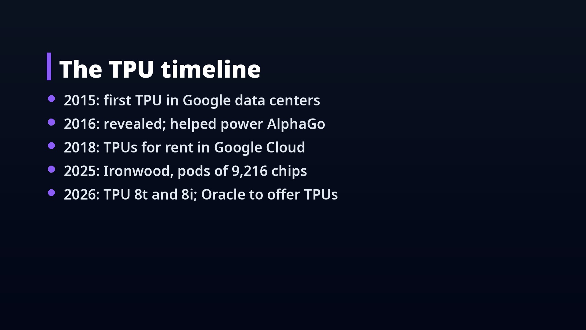
The TPU timeline marks the shift: 2015 first TPU in Google data centers, 2016 revealed and powering AlphaGo, 2018 TPUs for rent in Google Cloud, 2025 Ironwood with pods of 9,216 chips, and 2026 TPU 8t and 8i with Oracle set to offer TPUs in its cloud.
The TPU timeline
GPU vs TPU Architecture: Cores vs Systolic Array
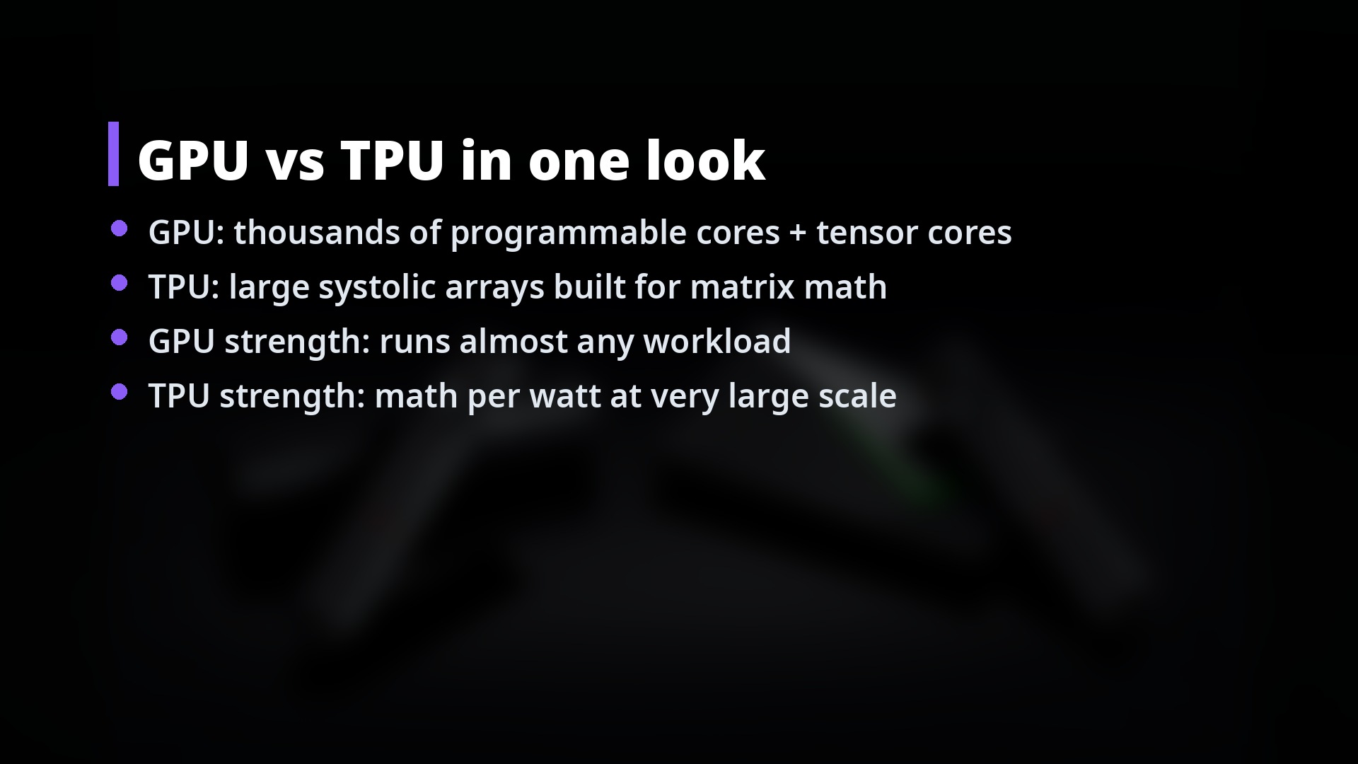
Almost all of modern AI comes down to one operation: multiplying big grids of numbers and adding up the results. A GPU attacks that with thousands of small, programmable cores. Picture a giant restaurant kitchen with thousands of cooks. Each one can make any dish, so the kitchen can handle any menu. That flexibility is why the same Nvidia chip can train a chatbot, render a film, or simulate a molecule. Modern Nvidia GPUs also carry tensor cores, special units built for exactly this grid math.
A TPU makes the opposite bet. Its heart is a systolic array: a grid of simple multiply-and-add cells wired to their neighbours. Think of an assembly line instead of a kitchen. Numbers enter at the edge and pulse through the grid, cell to cell, like a heartbeat. Each number is fetched once and reused many times on its way through, so the chip spends its energy on math, not on fetching. The trade-off is simple: the GPU is a generalist, the TPU is a specialist, and neither one is magic.
GPU vs TPU in one look
Memory Bandwidth Bottleneck: HBM, TPU 8i vs Rubin
Here is the part most comparisons skip. For chatbots, the math is often not the limit. Memory is. When a model writes a reply, it produces one token at a time, roughly a piece of a word. And for every single token, the chip has to read the model’s weights from memory again.
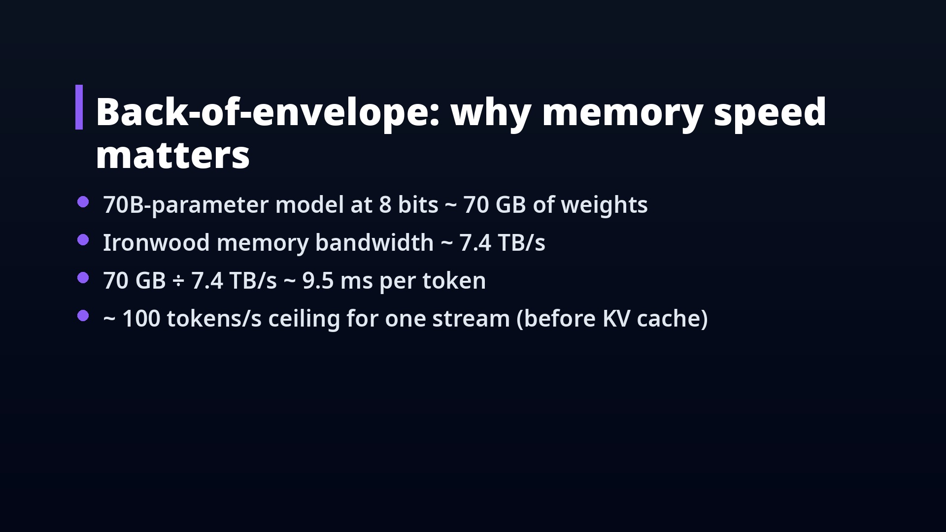
Take a model with seventy billion parameters, stored at eight bits each. That is about seventy gigabytes of weights. Google’s Ironwood TPU reads its memory at about seven point four terabytes per second. Divide one by the other, and you get a ceiling of roughly a hundred tokens per second for a single conversation. The calculation steps: 70B parameters × 8 bits = 70 GB of weights; Ironwood memory bandwidth ≈ 7.4 TB/s; 70 GB ÷ 7.4 TB/s ≈ 9.5 ms per token; ≈ 100 tokens/s ceiling for one stream before KV cache (Google Cloud, Hot Chips).
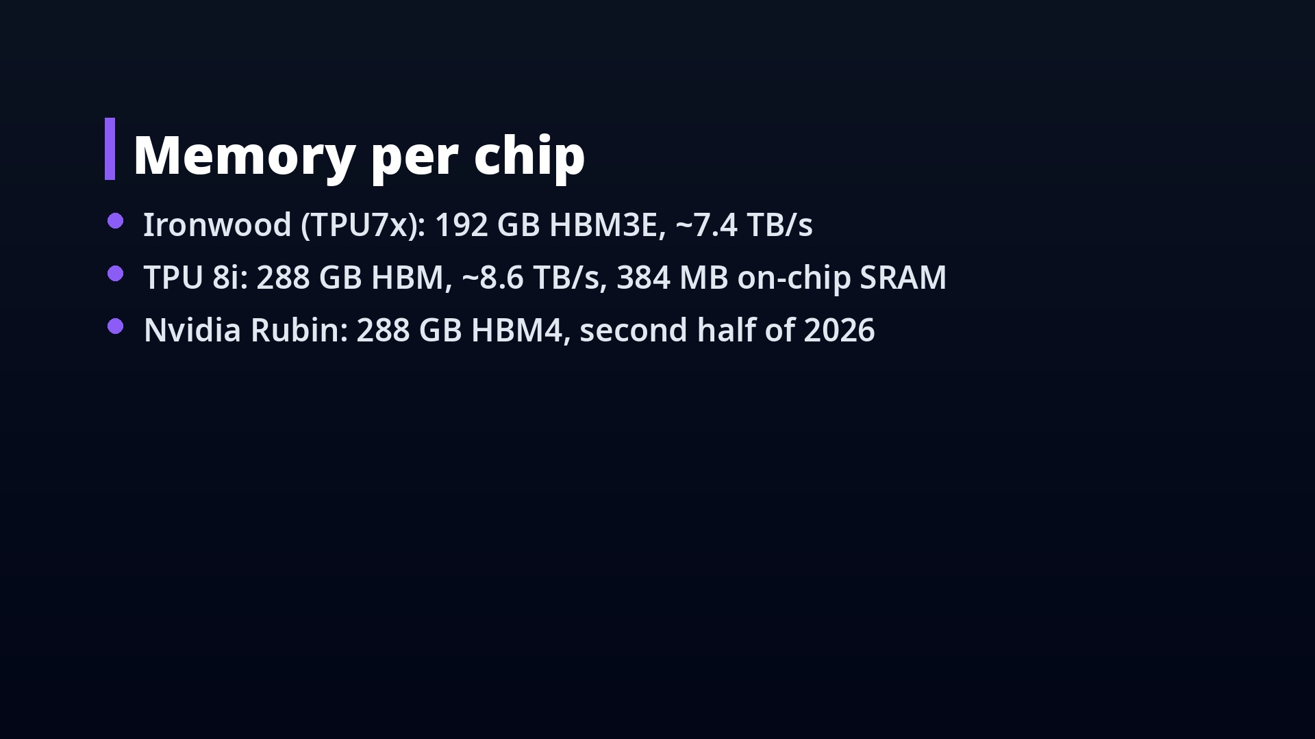
The trick is batching. Serve many users at once, and one trip to memory feeds all of them. That is why the newest chips compete on memory, not just on raw math. Ironwood carries 192 gigabytes of high-bandwidth memory. Google’s new inference chip, TPU 8i, raises that to 288 gigabytes, plus a large on-chip cache of 384 MB SRAM and ~8.6 TB/s bandwidth (Techzine). Nvidia’s next generation, Rubin, also brings 288 gigabytes per GPU on newer HBM4 memory, shipping in the second half of 2026 (DatacenterDynamics).
Back-of-envelope: why memory speed mattersMemory per chip
TPU Pods vs Nvidia NVLink Racks: Scaling Up
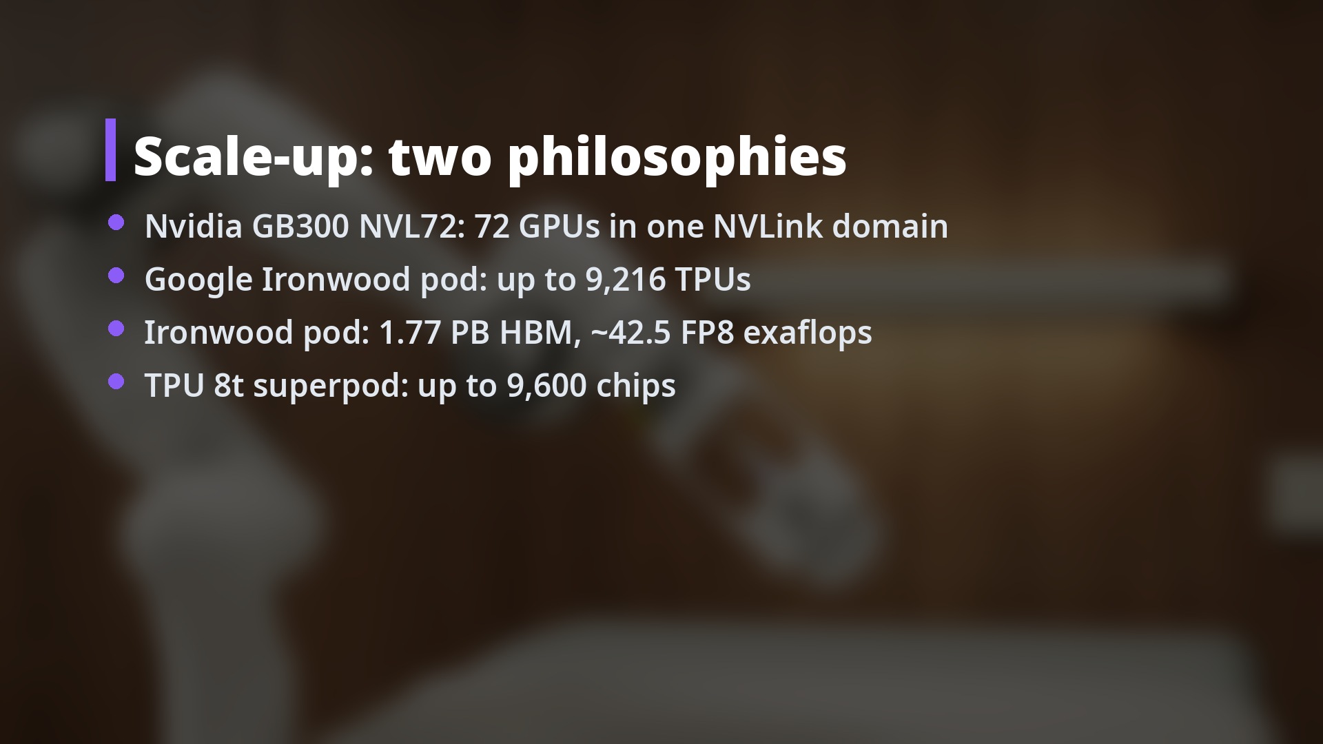
The biggest models do not fit on one chip, so the real product is a huge group of chips acting as one computer. Nvidia’s answer is the rack: seventy-two Blackwell GPUs joined by NVLink into one fast domain, then racks linked by networking (source: reference). Google’s answer is the pod. An Ironwood pod links up to nine thousand two hundred and sixteen chips. They connect in a three-dimensional mesh, and optical switches can reroute the links with tiny mirrors, working around a failed chip.
According to Google, one full pod holds 1.77 petabytes of high-bandwidth memory and about forty-two exaflops of eight-bit compute (Hot Chips). Which design wins depends on the job. Giant training runs love pods, while racks are easier to buy and drop into almost any data center. There is also an ownership difference. You can buy Nvidia racks for your own data center, if it has the power and liquid cooling. TPUs are almost always rented as a cloud service. Even Oracle will offer them that way, and only giants like Meta reportedly run them on site. TPU 8t superpods scale to 9,600 chips (Techzine).
Scale-up: two philosophies
CUDA Moat vs PyTorch on TPU: TorchTPU, vLLM
If TPUs are so efficient, why does Nvidia still sell most of the world’s AI chips? Software. Since 2006, Nvidia has built CUDA, the layer that lets programmers put its GPUs to work (source: reference). Nearly every AI library, tutorial, and research codebase assumed CUDA, so switching chips meant rewriting and re-testing code. Google’s own teams use JAX and the XLA compiler, which fit TPUs naturally. That is how Gemini is trained. But most of the world writes PyTorch.
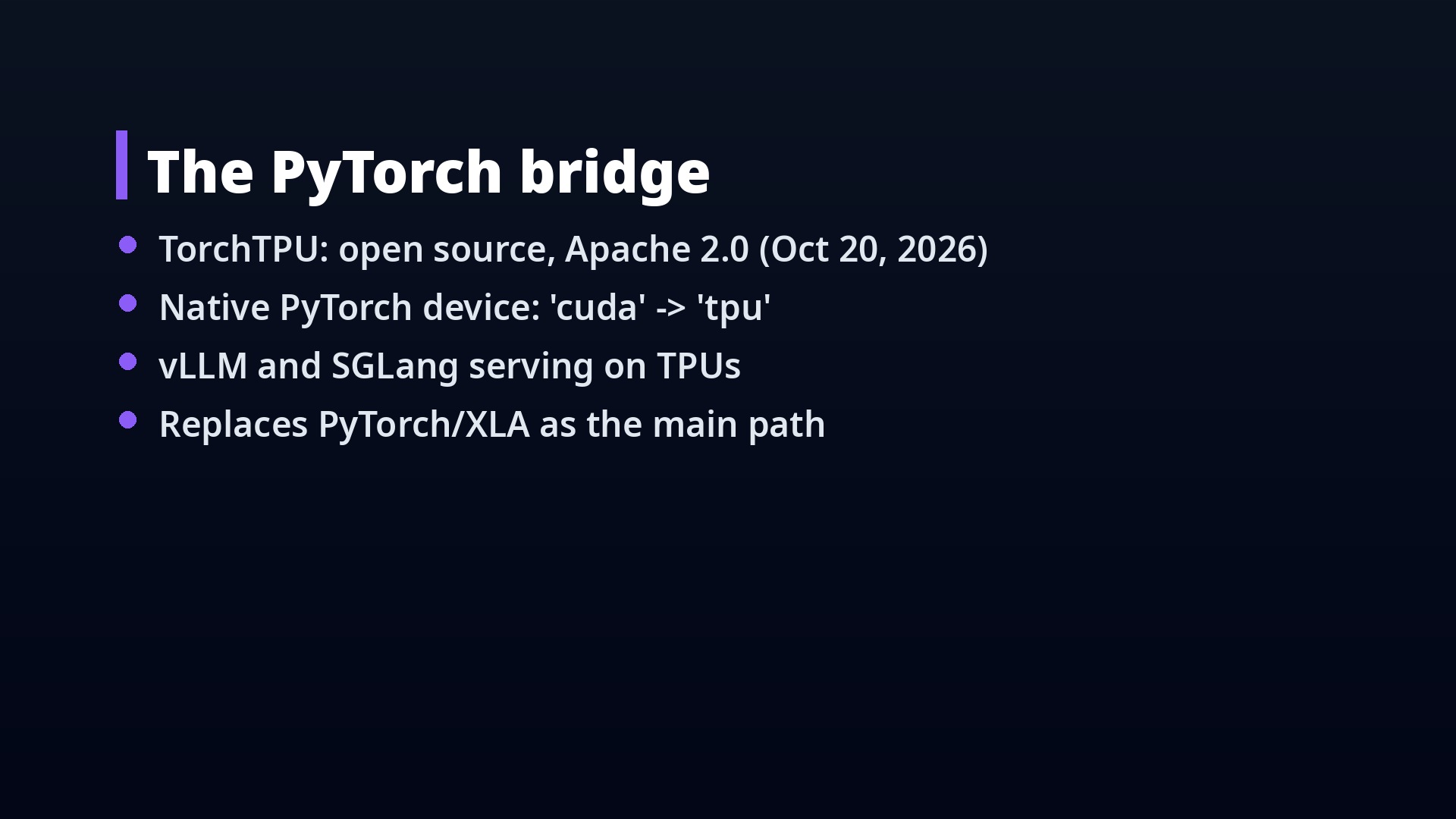
On October twentieth, 2026, Google open-sourced TorchTPU, built together with Meta’s PyTorch team. It makes the TPU a native PyTorch device (Google Developers Blog). In many cases, moving code means changing the device name from ‘cuda’ to ‘tpu’. The serving engines vLLM and SGLang run on TPUs too, and Meta says its SGLang setup on TPUs is already in production (LMSYS). The moat is not gone. Hand-tuned CUDA code does not move by itself. But the bridge is real now. TorchTPU is Apache 2.0 licensed and replaces PyTorch/XLA as the main path.
The PyTorch bridge
Who Buys TPUs: Anthropic, Meta, Apple, Oracle
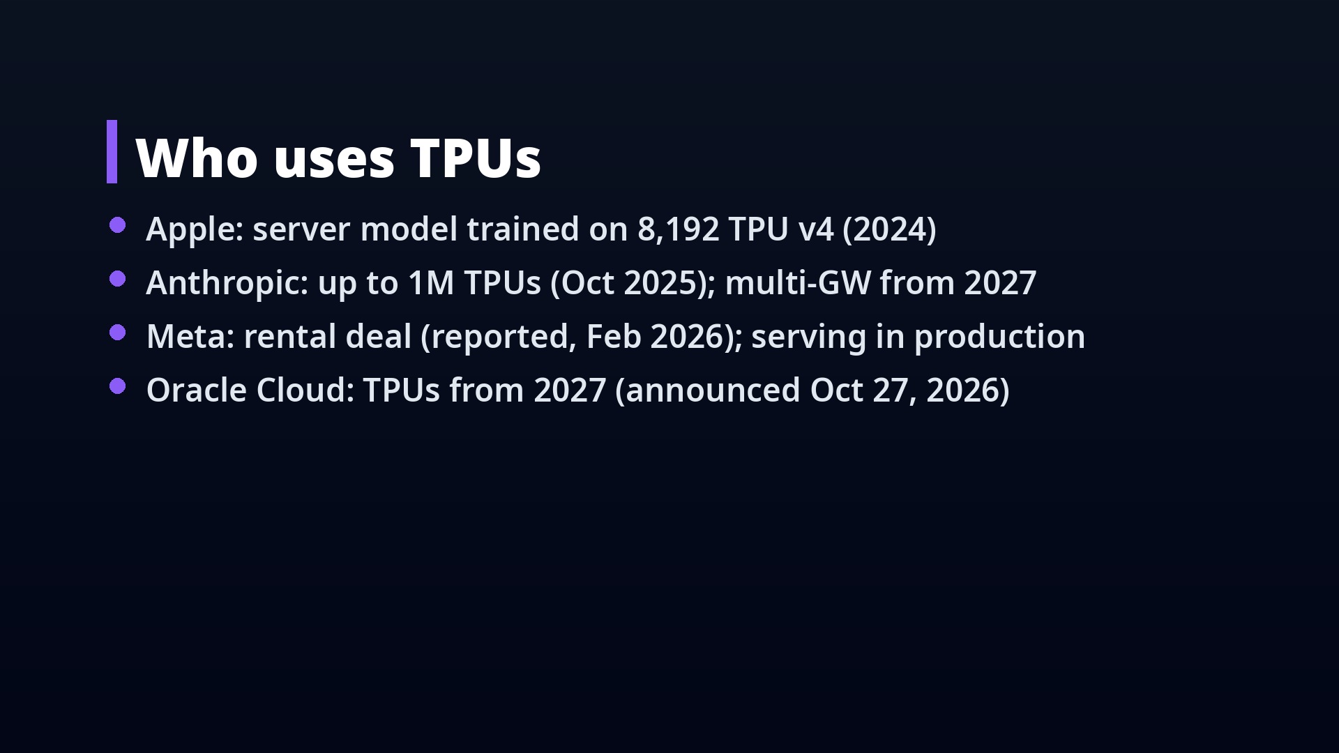
Customers tell this story better than benchmarks. Apple’s 2024 technical report says its server foundation model was trained on more than eight thousand TPUs—specifically 8,192 TPU v4 chips (Apple). In October 2025, Anthropic, the maker of Claude, announced it would use up to one million TPUs, a deal reported at tens of billions of dollars, bringing well over a gigawatt online in 2026 (Anthropic).
In April 2026 it went further: multiple gigawatts of next-generation TPU capacity with Google and Broadcom, starting in 2027. Broadcom, which co-designs the chips with Google, put that at about three and a half gigawatts (The Next Web). Meta reportedly signed a multi-billion-dollar deal in February 2026 to rent TPUs, and now runs some of its serving on them (Free Malaysia Today). And Oracle will offer TPUs in its own cloud from 2027, the first time Google’s chips run in another hyperscaler’s cloud (SiliconANGLE).
But notice something. None of them is quitting Nvidia. Weeks after its TPU deal, Anthropic committed thirty billion dollars to Microsoft Azure capacity on Nvidia systems, and Amazon remains its primary training partner (constellationr.com). Big AI labs buy several kinds of chips, for price, for supply, and for bargaining power.
Who uses TPUs
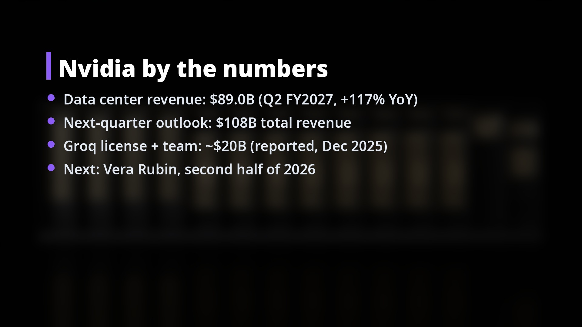
Nvidia’s Answer: Rubin, Groq and $89B
Nvidia noticed. In November 2025, Google released Gemini 3, trained on TPUs, and reports of Meta’s TPU talks hit Nvidia’s stock. Nvidia replied in public. It said it was delighted by Google’s success, then added that it is a generation ahead of the industry (Tom’s Hardware). On Christmas Eve 2025 it licensed technology from Groq, an inference-chip startup, and hired its founder Jonathan Ross, who helped start the TPU at Google. Reports put that deal at around twenty billion dollars (constellationr.com).
And the business is still enormous. In the quarter that ended in July 2026, Nvidia’s data center revenue was eighty-nine billion dollars, up one hundred and seventeen percent in a year; total revenue ninety-six point two billion; Q3 outlook one hundred eight billion (SEC). So this is not a story of Nvidia collapsing. It is a story of a market now big enough for a serious second option. Next up: Vera Rubin in the second half of 2026.
Nvidia by the numbers
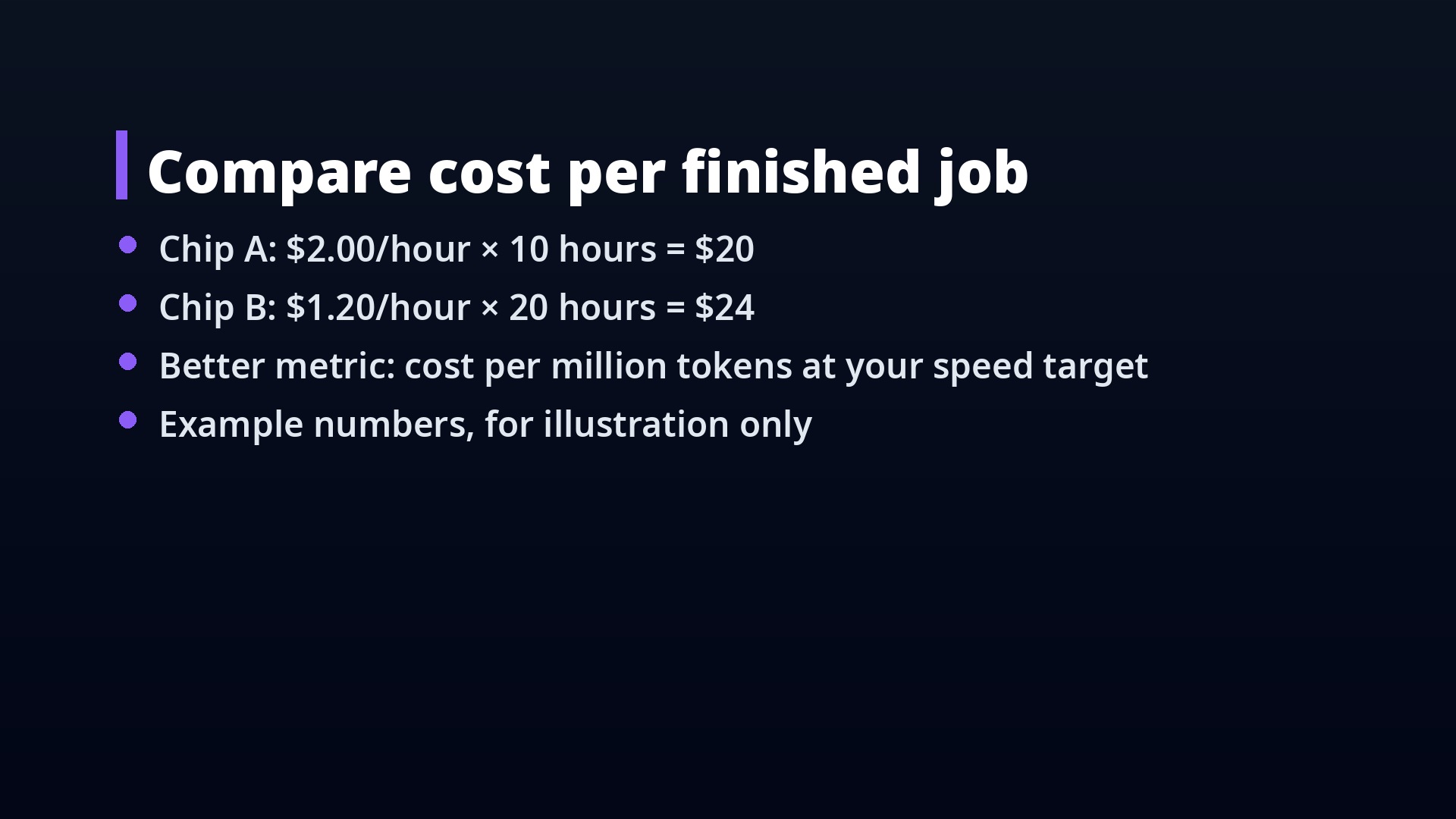
AI Chip Cost: Hourly Price vs Cost per Token
Now the question that matters to anyone paying the bill: which chip is cheaper? The honest answer is that the hourly price tells you almost nothing. Imagine chip A rents for two dollars an hour and finishes a job in ten hours. That is twenty dollars. Chip B rents for one dollar twenty, but needs twenty hours. That is twenty-four dollars. The cheaper chip costs more.
Watch the fine print, too. When Google says TPU 8i gives eighty percent better performance per dollar, it compares against its own previous TPU, not against Nvidia. So test your own model: same quality, same response time, then compare the cost per million tokens and the engineering hours to move it. Measure utilization too. A cheap chip that sits idle half the time, waiting for data or restarting failed jobs, really costs double. And price the move itself: weeks of engineers porting and re-testing code can erase months of savings. And count availability. The best chip is useless if you cannot get capacity when you need it.
Compare cost per finished job
Try a TPU for Free (Kaggle, Colab) + Who Wins
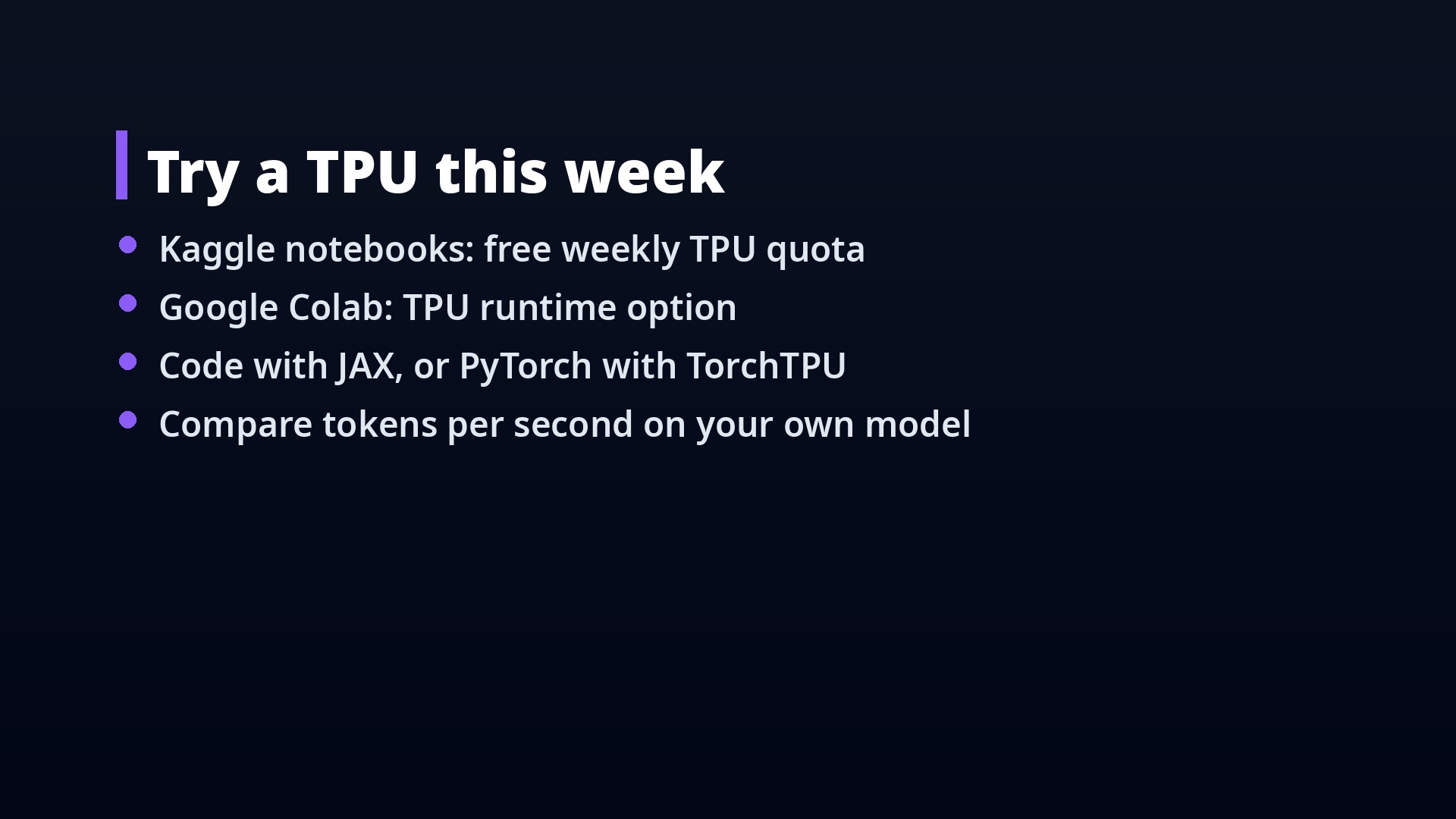
You do not need a million chips to try this. Kaggle notebooks come with free TPU time every week—about twenty hours—and Google Colab offers TPU runtimes too (Google Cloud). Run the same small model on a GPU and on a TPU, and compare the speed yourself. Code with JAX, or PyTorch with TorchTPU.
So, can Google beat Nvidia? Not by replacing every GPU. Google wins if TPUs become the obvious second choice: for giant training runs, for cheaper answers at scale, and now in other clouds. Nvidia wins as long as it stays the easiest place to start and the fastest place to run the newest models. For the rest of us, real competition means cheaper AI and more choice. That is the actual win.
Try a TPU this week
FAQ
What is the main architectural difference between a TPU and a GPU?
A GPU uses thousands of programmable cores plus tensor cores for flexibility across workloads. A TPU uses a systolic array—a grid of simple multiply-add cells wired to neighbors—so data flows through once and is reused, optimizing math per watt for large-scale matrix operations.
Can I run PyTorch models on TPUs today without rewriting code?
Yes. Since October 20, 2026, Google’s open-source TorchTPU (Apache 2.0) makes TPUs a native PyTorch device. In many cases you only change the device string from ‘cuda’ to ‘tpu’. Serving engines vLLM and SGLang also run on TPUs, and Meta reports production use.
Which is cheaper: renting TPUs or GPUs for inference?
Hourly price alone is misleading. The real metric is cost per million tokens at your target latency and quality. A cheaper chip that runs slower or sits idle can cost more per finished job. Test your specific workload, including engineering effort to port and utilization rates, before deciding.
Competition between Google and Nvidia is expanding the menu of AI compute—giving engineers more leverage, better pricing, and a reason to benchmark instead of defaulting.
Ali YAZICI is a Senior IT Infrastructure Manager with 15+ years of enterprise experience. While a recognized expert in datacenter architecture, multi-cloud environments, storage, and advanced data protection and Commvault automation , his current focus is on next-generation datacenter technologies, including NVIDIA GPU architecture, high-performance server virtualization, and implementing AI-driven tools. He shares his practical, hands-on experience and combination of his personal field notes and “Expert-Driven AI.” he use AI tools as an assistant to structure drafts, which he then heavily edit, fact-check, and infuse with my own practical experience, original screenshots , and “in-the-trenches” insights that only a human expert can provide.